


Aluminum nitride, silicon nitride, ceramic substrates.
In the new energy and next-generation communication industries, with the rapid development of microelectronics information technology, large-scale integrated circuits (LSI), multi chip modules (MCMs), and microelectromechanical systems (MENS), the requirements for electronic complete machines are becoming increasingly high, and this demand is becoming increasingly urgent, promoting their development towards miniaturization, portability, high-performance, and other directions. High density integration is the most effective solution to achieve the above functions. High density integration can integrate the complex functions of various electronic devices into smaller components, and the key to achieving high-density integration is to solve the heat dissipation problem of components. For electronic devices, the effective lifespan of the device is usually reduced by 30% to 50% for every 10 ° C increase in temperature. Therefore, selecting appropriate packaging materials and processes to improve the heat dissipation ability of devices has become a technical bottleneck in the development of power devices.
Taking high-power LED packaging as an example, due to the conversion of 70% to 80% of input power into heat (only about 20% to 30% converted into light energy), the small area of LED chips, and the high power density of devices (greater than 100W/cm2), heat dissipation has become a key issue that must be solved in high-power LED packaging. If the chip heating cannot be exported and dissipated in a timely manner, a large amount of heat will accumulate inside the LED, and the chip junction temperature will gradually increase. On the one hand, it will reduce the LED performance (such as reduced luminous efficiency and wavelength redshift), and on the other hand, it will generate thermal stress inside the LED device, causing a series of reliability issues (such as service life, color temperature changes, etc.).
With the continuous development of power devices (including LED, LD, IGBT, CPV, etc.), using high thermal conductivity materials to make circuit substrates is one of the effective methods to achieve microcircuit heat dissipation.
Currently, commonly used electronic packaging substrates can be divided into polymer substrates, metal substrates (metal core circuit boards, MCPCBs), and ceramic substrates. For power device packaging, in addition to basic wiring (electrical interconnection) functions, the packaging substrate also requires high thermal conductivity, heat resistance, insulation, strength, and heat matching performance. Therefore, the use of polymer and metal substrates is greatly restricted; Ceramic materials themselves have high thermal conductivity, good heat resistance, high insulation, high strength, and thermal matching with chip materials, making them very suitable as packaging substrates for power devices. Currently, they have been widely used in fields such as semiconductor lighting, laser and optical communication, aerospace, and new energy vehicles.
Aluminum nitride and silicon nitride ceramic substrates and their applications in new energy vehicles
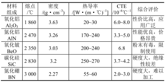
At present, the main materials for ceramic substrates are aluminum oxide (Al2O3), aluminum nitride (AlN), and silicon nitride (Si3N4). Aluminum oxide ceramic substrate has a low price, mature production process, and currently has the largest output and widest application range. However, the thermal conductivity of alumina ceramic substrates is no longer sufficient to meet the heat dissipation requirements of high-power chips. Overall, aluminum nitride ceramic substrates and silicon nitride ceramic substrates have the most promising development prospects.
Comparison of Characteristics of Some Ceramic Materials
Aluminum nitride substrate
Aluminum nitride ceramics have excellent performance, especially their high thermal conductivity. Their theoretical thermal conductivity can reach 320W/(m · K), and their commercial products generally have thermal conductivity ranging from 180W/(m · K) to 260W/(m · K), making them suitable for high-power, high lead, and large-size chip packaging substrate materials.
In addition, aluminum nitride ceramics also have high mechanical strength and chemical stability, which can maintain normal working conditions in harsh environments. It is precisely because aluminum nitride ceramics have many excellent properties that they will stand out among numerous ceramic substrate materials and become a representative product of the new generation of advanced ceramic packaging materials.
The working temperature of car LED headlights is extremely high. The higher the power, the higher the temperature, and the brightness power is proportional. To improve the brightness, it can only be achieved through precise cooling design or increased heat dissipation devices, but the effect is not ideal. Only aluminum nitride ceramic substrate can achieve the desired effect. The advantages of high thermal conductivity, excellent insulation, and thermal expansion technology that better matches the lamp beads have once again made aluminum nitride ceramic substrates stand out.
Silicon nitride substrate
Silicon nitride is considered to have the best comprehensive performance as a ceramic substrate material. Although its thermal conductivity is not as good as aluminum nitride, its bending strength and fracture toughness can reach more than twice that of aluminum nitride. Meanwhile, the thermal expansion coefficient of silicon nitride ceramic substrate is similar to that of third-generation semiconductor silicon carbide, making it the preferred material for silicon carbide thermal conductive substrate. The application of silicon nitride substrate in new energy vehicles is unstoppable!
(1) IGBT
The core component of the electric motor drive part of new energy vehicles is the IGBT. IGBT accounts for about half of the cost of motor drive systems, while motor drive systems account for 15-20% of the total vehicle cost, which means IGBT accounts for 7-10% of the total vehicle cost. It is the second most expensive component besides batteries, and the quality of IGBT largely determines the energy efficiency of the entire vehicle.
The full name of IGBT is insulated gate bipolar transistor. The power conductive terminals of IGBT modules used in electric vehicles need to carry a large current of hundreds of amperes, and have high requirements for conductivity and thermal conductivity. They also need to withstand certain vibration and impact forces in the vehicle environment, with high mechanical strength requirements. In recent years, Si3N4 ceramic substrates have been favored in IGBT module packaging due to their excellent properties such as high hardness, high mechanical strength, high temperature resistance and thermal stability, low dielectric constant and dielectric loss, wear resistance, corrosion resistance, etc., and are gradually replacing Al2O3 and AlN ceramic substrates.
(2) SiC MOSFET
With the continuous development of technology and the extension of application needs, the limitations of the first and second generation semiconductors have gradually become apparent, making it difficult to meet the needs of high-frequency, high-temperature, high-power, high-energy efficiency, harsh environment resistance, and lightweight miniaturization. The third-generation semiconductor materials represented by silicon carbide (SiC) and gallium nitride (GaN) have the characteristics of large bandgap width, high critical breakdown voltage, high thermal conductivity, and high carrier saturation drift rate. The electronic devices produced by them can work stably at temperatures of 300 ℃ or even higher.
In the core motor drive of new energy vehicles, the use of SiC MOSFET devices brings a 5% to 10% increase in endurance compared to traditional Si IGBTs, and will gradually replace Si IGBTs in the future. However, SiC MOSFET chips have a small area and high requirements for heat dissipation. Silicon nitride ceramic substrates have excellent heat dissipation ability and high reliability, making them almost a necessary option for the main drive application of SiC MOSFETs in the field of new energy vehicles.
At present, the Tesla model 3 that has been mass-produced has used silicon nitride ceramic substrates in large quantities to cope with the heat dissipation of SiC MOSFET devices. The new generation of SiC electronic control launched by BYD e3.0 platform adopts a self-developed new SiC MOSFET motor control module, high-performance silicon nitride ceramics, and integrated NTC sensors, which increases the power density of the entire electronic control unit by nearly 30%. The maximum current support is 840A, the maximum voltage is 1200V, and the maximum efficiency of electronic control is 99.7%.
AMB ceramic substrate will become the mainstream process for heat dissipation in mid to high-end power modules
Ceramic substrates are mainly divided into DPC, DBC, AMB, LTCC, HTCC and other substrates according to the process.
AMB ceramic substrate is a further development of DBC technology, which uses solder containing a small amount of rare earth elements to connect the ceramic substrate to copper foil, with high bonding strength and good reliability.
The ceramic substrates produced by the AMB process are mainly used on power semiconductor modules as substrates for silicon based and carbide based power chips. AMB technology achieves the bonding of aluminum nitride and silicon nitride ceramics with copper sheets, which has better thermal conductivity, copper layer bonding force, reliability, etc. compared to DBC lining plates. This can greatly improve the reliability of ceramic lining plates and is more suitable for high-power and high current application scenarios, Gradually becoming the main application type for mid to high-end IGBT module heat dissipation circuit boards.
In addition, due to the high thermal conductivity of AMB silicon nitride substrate, very thick copper metal (up to 0.8mm in thickness) can be welded onto relatively thin silicon nitride ceramics, resulting in high current carrying capacity. Moreover, the thermal expansion coefficient of silicon nitride ceramic substrate is close to that of the third-generation semiconductor substrate SiC crystal, making it more stable in matching with SiC crystal materials. Therefore, it has become the preferred material for SiC semiconductor thermal conductive substrate, especially in the application of high-end new energy vehicles above 800V.
According to the QY Research report, the market size of AMB ceramic substrates in 2021 was approximately $90 million, and it is expected to grow to $380 million in 2028, with a compound growth rate of up to 22.7%.
Post time: Aug-29-2023